A Homebrew S-100 Bus System Monitor (SMB) Board Introduction Most S-100 users
that like to work with hardware have some kind of front panel or hardware
monitor for their system. It allows
you to see what was "going on". Often in a very general sense but
in the case of
systems that can "single step" and/or display the bus memory and data lines
they can be very useful indeed for debugging.
The gold standard was the IMSAI front panel. Beautifully done but
unfortunately setup for old S-100 systems with little ability to give
meaningful information with high speed/extended addressing for later S-100 systems.
In my opinion the Intersystem's front panel was perhaps the best of
that era. However in the end, and for a number of reasons I decide to build
my own board. Initially it was in fact two boards with all chips point to point
connected with soldered wires. The project evolved. I kept adding more and
more functions. The Breakpoint and Single Step circuitry come directly from
Sol Libes & Mark Garetz's book "Interfacing to the S-100/IEEE 696
Microcomputers". A must have book BTW, for anybody doing S-100
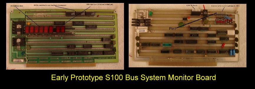
Computers hardware. Here is a picture of the early pair of SMB prototype board
pair:-
The board utilized HP 5082-7340 Hex display LED's to show the 24 bit data
address and 8 bit data being read by the CPU (a Z80) in real time. It had an
"IOBYTE port" (see below) for BIOS configuration and a 24 bit hardware
breakpoint switch. Because the board was point to point wired and
soldered it utilized two S-100 boards and connected to the front of my
computer box with LED's and switches via a ribbon cable and connector
As I utilized the board over the years I really appreciated its capability
to tell me at all times where and what the (master) CPU was doing.
Nevertheless as time went by I started to think of further additions and
improvements to the board. The board described below is the
result of these considerations. Here is a picture of the board. Let me
briefly outline first the components of the board.
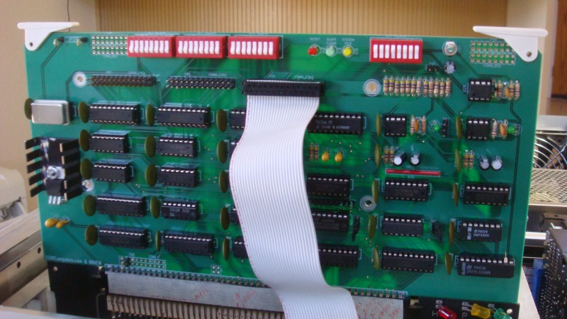
The SMB Board
This S-100 SMB board
has the following functions:-
Important S-100 Bus signals.
The following S-100 signals are brought out as LED's:-
Memory Read, Memory Write, Port In, Port Out,
Interrupt Acknowledge, Processor Halt, Phantom
RAM Addresses Greater than 64K, 16 Bit Data Request, Temporary Master 1 in
Control.
These signals can be brought out to the front of the computer box via a
ribbon cable connector or displayed on a daughter board attached to the
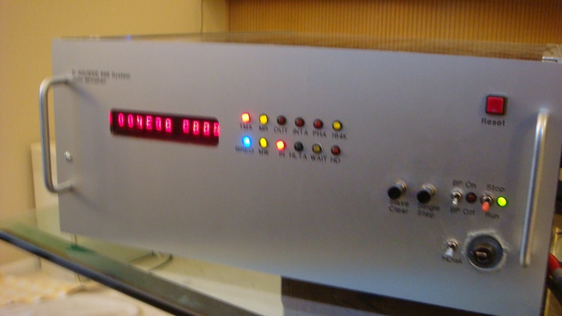
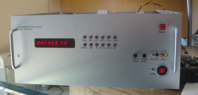
S-100 card (see below). Here is a picture of the front of
my system
displaying the above indicator LED's.
Please see here for a
description of a description of these important S-100 signals. By looking at these LED's you can
immediately see if an S-100 signal is "stuck" high or low. Active high
S-100 lines are red LED's, active low lines are green. Because
many of
the signals emit only a narrow pulse that would not be seen by the eye (for
example INTA), the board uses a number of 74LS123 "single shots" to stretch
the light pulse time so they are visible.
HEX LED display of all Data and
Address lines. At all times the
address of the master (or slave) CPU's program counter is displayed as a Hex
LED display. If an 8 bit CPU is controlling the bus the current 8 bit
instruction it is reading is displayed. If a 16 bit CPU is
currently the master the 16 bit bidirectional data bus is displayed.
Note because most 16 bit CPU's pipeline their instructions the data in and
address bus may be slightly ahead of the actual instruction the CPU is
executing.
Hardware Breakpoint Switches.
The board has a row of 20 small dip switches and circuitry such that if the
CPU ever goes to a specified address it will stop. From there it can then be
single stepped forward one CPU instruction at a time displaying the current
24 bit address and 8/16 bit data in being read on the bus. This is very useful
for both hardware and software debugging. Unlike software debuggers it is
memory location and CPU type independent. It will work anywhere in the 24
bit S-100 memory address space with a master or any slave CPU.
Stop and Single Step Circuitry. This circuitry allows one to stop the
current running master CPU at any time and restart from that location again
or single step the CPU forward one instruction at a time.
Hardware Reset and Slave Clear
Circuitry. In the past I have
had problems with the length of time a low going reset signal was presented
on the bus. For example the SD Systems 8024
Video boardwill not reset its onboard CRT
controller in time if the signal is too short. It is also
important to have a single sharp square wave reset signal for CPU's like the
80286. Finally many older S100 CPU boards do not have a Slave Clear
option. For these reasons I have added two 555's to allow precise
control of the S-100 Reset and Slave Clear functions. These can be triggered
by push button switches.
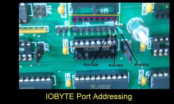
An IOBYTE Port.
This is a simple 8 bit switch/input port that allows the user to configure
the consol, printer reader etc for IO in hardware. It's a carry over
of the early Teletype days and was used in early versions of CPM, but it is
useful is setting BIOS options because the data is not lost when the power
is removed. The port can reside anywhere within the range of E8-EFH
Master/Slave Switching Circuitry. This
is an input port that allows one to bring low the S-100 TMA0 or TMA1 bus
lines, useful for CPU master/slave switching. The port can reside anywhere
within the range of E8-EFH
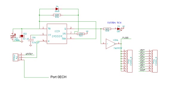
A System Tick Clock.
This is just a simple timer that allows one to pulse one of the S-100 interrupt
lines ~10 times a second. This is useful for CPM-86 background processing
and multi-user systems. Again a 555 time is used but the "normal"
circuitry
is modified (with a diode) to give a narrow sharp low going pulse which can
be jumpered to any one of the S-100 vector interrupt lines V0-V7. The clock
it reset by the S-100 INTA or by inputting from a port (one of E8H -EFH) via
a jumper.
A 2MHz signal for the S-100 Bus line
#49. This line is not often used
but when it is, it is typically used for things like a UART baud rate
generator. The IEEE-696 specs specify exactly and always 2MHz. Some older
S-100 boards tap into the master CPU clock (4MHz) and divide by two.
This limits these boards to being always used at 4MHz.
Inverse of the Master Clock signal
(S-100 line #25). Some older
S-100 boards count of the pSTVAL signal being a simple inverse of the main
clock signal. The IEEE-696 signal is not exactly like this. The
most well known example of this is the
SD Systems Versafloppy II FDC board. There are modifications that
can be made to that board to get it to work but the simplest thing to do is
just supply the inverse clock signal on an unused S-100 bus line and
redirect the Versafloppy to that line. I use the unused S-100 line
#27, "RFU".
The Circuitry.
Unlike most S-100 boards describe here the electronic circuitry on the board is really
quite simple. There is just a lot of it. All the indicator LED's or HEX displays
are driven by inverters.
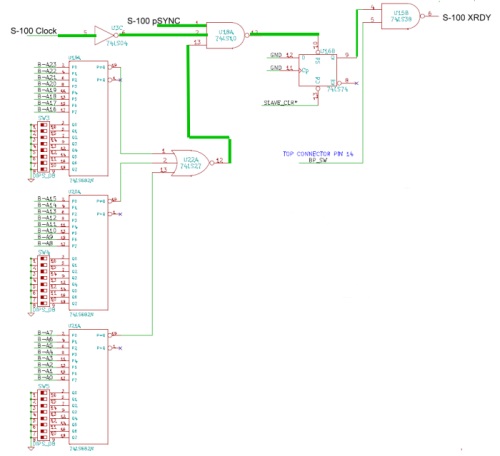
Here is a
full schematic of the board.
The board utilizes 74LS682's for port addressing. If your are unfamiliar
with this technique click
here.
The breakpoint circuitry is set by adjusting the top leftmost 3 eight
position dip switches to be 24 bit binary address you want the bus master
CPU to stop at. It does not matter if its an 8080, Z80, 8086, 80286... It
will stop the CPU if ever that address is accessed. The core of the
circuitry
is just three 8 bit comparators and a flip flop to latch the S-100 bus
XRDY line low.
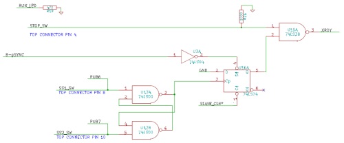
The Stop and Single Step circuitry is equally simple. Here it is:-
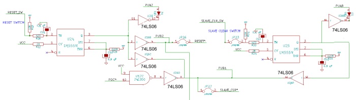
The 555 Reset and Slave Clear circuitry is shown here. Note Power On Clear
(POC) also brings low the slave clear line - something some boards do not
do:-
Finally here is the "System Tick" Interrupt clock circuitry:-
This simple circuit is used to generate a periodic pulse for an interrupt
for things like CPM-86's interrupt driven system. It can be used as a
CPM "poor man's" real time clock (the trim cap lets you fine tune the
system) but I am currently doing a full blown PIC (Priority Interrupt
Controller) and Clock/Calendar S-100 board which will eventually replace
this component.
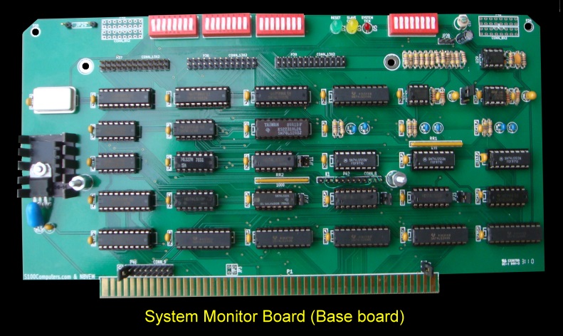
With Andrew (see below) we collected all of the above and a few other things
and squeezed them all on to one board.
Here is a picture of the
prototype board:-
In my second (testing S-100 system), I do not have a front panel box to
house the S-100 boards. In this system I attach the HEX displays (see
below), LED's and switches on a small daughter board that is piggy backed on
to the main S-100 board as shown here:-
The 10 HP 5082-7340displays
are excellent displays for presenting the address lines and Hex data on 8
bit lines. They have their own internal circuitry to convert 8 bits into an
HEX character 0-F. Unfortunately these displays are now fairly hard to find
and somewhat expensive (typically $8-$12 each on eBay). Most modern similar
displays unfortunately only decode 8 bits from 0 to 9!
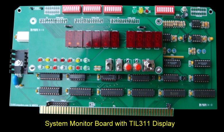
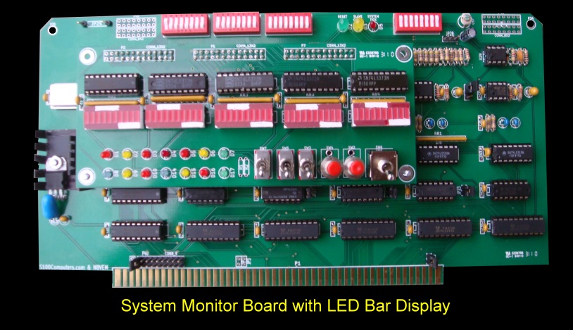
Understanding that not everybody would want such a luxury, Andrew and I have decided to make three versions of the board. In
all three cases
the actual LED display itself is on a small daughter board that attaches to the front
of the single main S-100 board. One daughter board is designed to accept the
above HP 5082-7340HEX displays.
Another board (exactly the same dimensions) will accept the common bar graph
LED's. These work by displaying the 24 address and 8/16 data lines as binary bits.
There is still another daughter board for the somewhat easier to find (and
cheaper) TIL 311 HEX displays. All three daughter boards also contain the necessary switches to stop, reset and
single step etc. the CPU.
In my case (and I'm sure for others) I wanted to bring out the HEX display
and switches to the front panel of my S-100 box. To allow this, the board
has a three ribbon cable connectors which connect directly to the switches
and HEX displays.
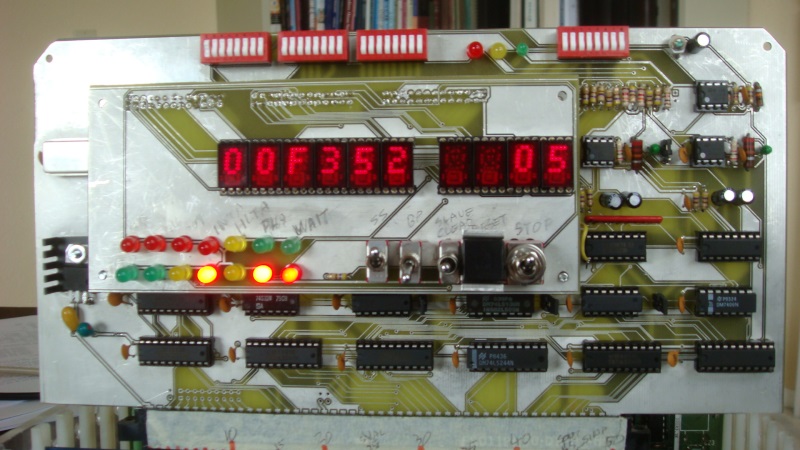
A Second Prototype.
A second prototype board was done to improve on some of the functions of the
first board. Here is a picture of that board.
As you can see it almost the same as the first board but has a few minor
corrections and is constructed on a commercial layout/material.
Construction of a final board is now under way.
The S-100 Bus SMB in Action:-
The short (amateur) video below shows the S-100 SMB board in action. The system
is powered up. CPM-80 is first booted from the
IDE S100 Board. Then CPM-86
is then booted from the same IDE board. I then stop the CPU and single
step along the 8086 one instruction at a time. You can see the address and
16 bit data lines being displayed. I then reset the computer and do the same
thing with the Z80.
To play the video click on the arrow within the
window.
(Note: You must have Adobe Flash installed on your computer to
see this video. You can download the latest Adobe Flash
Player for your Browser
here).
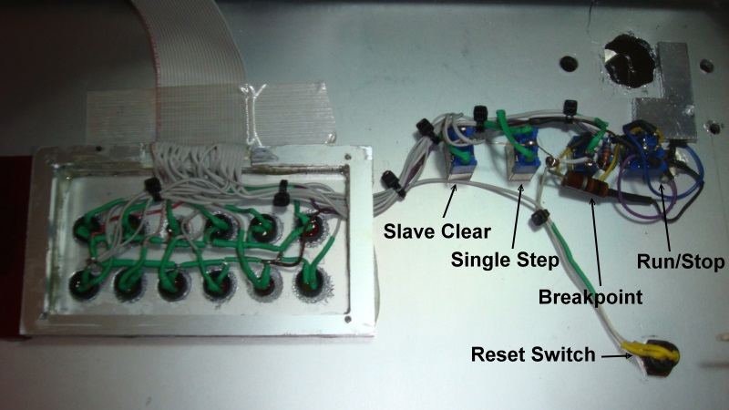
External LED's
and Switches
In my main S-100 system, which is a custom hand built box, I have brought
the bus indicator LED's out to the front panel of the box. I also relocated
the HEX display LED's to a small window cut into the front of the box.
Finally the switches were also brought to the front of the box. This
required that three 26 conductor ribbon cables with sockets be connected to
the board. Below are a few pictures of my construction process.
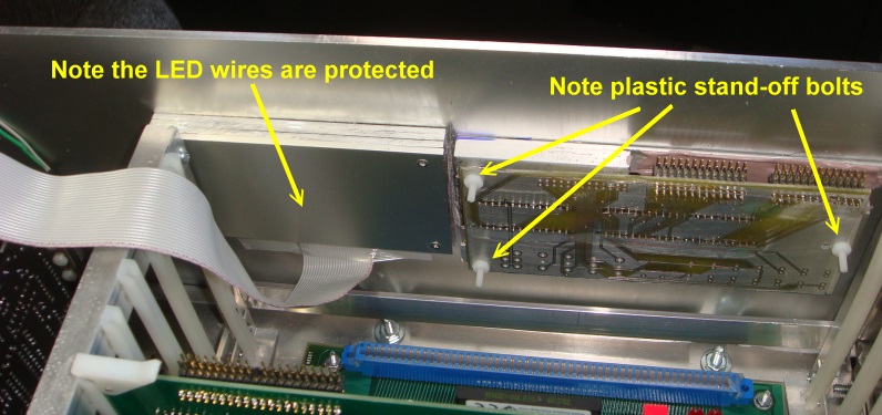
It is obviously very important to make sure all wires are insulated and not
exposed. The LED's tend to be fragile and the wires can break over time. For
this reason they are enclosed in their own "Box", sealed and covered.
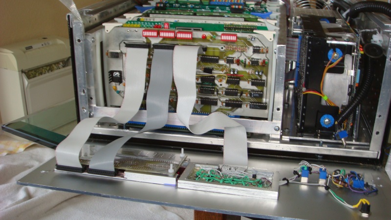
Below is a picture of the complete
set-up before the front panel is re-attached to the system.
Below shows the final arrangement.
A Production S-100 Board.
Realizing that a number of people might want to utilize a board like this
(and the fact that I have 2 other S-100 systems that could use one) together
with Andrew Lynch at N8VEM (see
here) we have
just completed of laying out a "proper" commercial type S-100
board. Through Andrew's magic hands (and hard work) a very nice S-100 board
has emerged. If
you have an interest in such a bare board, let Andrew or I know. This
clearly applies only to people who know what they are doing and can do
a little soldering and board assembly. There would be little hand holding
at this stage.
Assembly Notes for those constructing
the board.
Assembly of the board is fairly straightforward. That said, here are some
useful hints:-
While the logic on the board is simple there is a lot of it. The traces on
the board are narrow and closely spaced. Take care not to scratch the board
when soldering connections. The solder mask on the board is excellent so
there should not be a problem. In splitting apart the three display
boards take care in cutting the small connecting bridges not to damage the
nearby traces. When soldering in caps and resistors, after
placing them in the board, solder in one side first for all then the other
side. This way the component has time to cool.
All components can be commonly obtained. I obtained mine from Jameco (except
the 74LS682's unfortunately -- which I use a lot and got as a batch from
DigiKey). Here are Jameco catalogue numbers of some components:-
1.5A, 5Volt voltage regulator
#924570
2MHz Oscillator #27924
TIL 311 displays #32951
10 Bar LED Display #697477
470 Ohm Resistor pack #97869
1K Ohm Resistor pack #78777
Trimmer Cap #32839
Dual Row jumper headers #67821
Single Row Jumpers (cut to size) #527654
Bypass capacitors #25525
Note, this is not a complete list.
First solder in all IC sockets, resistors, capacitors and jumper sockets.
You should use a 1.5A, 5V voltage regulator. The TIL and HP displays use a
fair amount of power. I like to keep my voltage regulators (and
boards) cool, so I used a somewhat larger heat sink. In order for it to fit
I had to drill a hole in it left of center. This way I could actually place
one cooling fin within the larger one. See below. Make sure the
cooling fins do not contact the add-on display board. See the picture above.
Before you add any IC's place the board in your system. Check it starts up
normally. If not find the solder bridge.
Next add the Voltage regulator and the U29 555. This is the system tick
circuitry. Insert the D5 LED and check that it flashes rapidly (1-3 times a
second). Make sure you have the LED polarity correct. The longer lead
to the square pad. Jiggle them around to check before soldering them in.
Then add the other two 555's (U24 & U25) as well as U17 and U26. Also
LED's D2 and D3. Insert jumpers JP27 and JP23. Then carefully
touch the connector P39 pin 12 (RESET_SW) or pin 18(SLAVE_CLEAR_SW) to
ground. The system should reset (pin#12) and the appropriate LED's should
come on briefly.
Next we will add the IOBYTE circuitry Input port address and Master/Slave
switch circuitry. We will do this in stages. First add the bus drivers,
U8,U9,U11,U12,U13 and U14 (do not add U28). Place the card in the bus and
check the system is OK. Next add U18,U3,U27 and U28 and switch SW9 if it is
already not there. We will input data from the switch settings from a
port in the range (E8H to EFH). You can choose your own. I will use port EFH
as the IOBYTE port (EDH as the master/slave switch (see below) and port EEH
to reset the timer tick (see below). To do this we need to carefully
jumper connections between connector P42 and K1 (both are side by side).
I prefer to use wire wrap connections with a wire wrap tool but solder
connections are also fine. Here is an enlarged picture:-
After you have setup the above connections insert the board in your system
and input from port EF. The value returned should reflect the switch
settings of switch SW9. Normally they are closed returning a value of 0FFH.
You can use various bits to redirect your BIOS outputs as discussed above.
There is circuitry on this board to control the S-100 TMA0 and TMA1 lines.
These are used to switch in other bus CPU's such as an 8086. We will use
them later with future boards. For now insert U2 and U15. Inputting
from port EDH should bring the S-100 line #55 low. (The connection for
port EEH is to reset the system tick when utilized with interrupt driven
systems like CPM86).
Next insert all the rest of the IC's on the board. Assemble the display
board. Be sure to get the polarity of the LED's correct. If in doubt don't
solder them in yet. Just tape them in and we will jiggle them around. Attach
the Display Board. Take care to make sure the back side of the display board
is not contacting anything on the S-100 board itself. Insert in your
system. Check that the appropriate LED's are lighting up correctly. For
example inputting from any port should flash the PORT IN LED. Placing 76H in
RAM and jumping to that address should cause the HALT LED to stay on.
Next check the Single Step circuitry as I described in the above video.
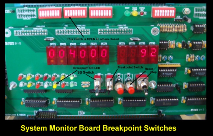
Finally you can test the hardware breakpoint circuitry. Setup the board
breakpoint switches so that all are closed except the one shown here in the
picture.
Flip the Breakpoint switch up and reset your system. Then display memory
from say 3F00H to 4100H. The computer will stop as shown above at address
4000H. Flip the Stop switch up. Then lower the Breakpoint switch. Then by
flipping the Single Step switch up and down you can step (the current S100
CPU bus master), one opcode at a time from this location. What
is nice about this arrangement is that it is software independent and will
work with any CPU anywhere in the 16MG address space of the S-100 Bus.
There are a few jumpers on the board to add flexibility for different
systems:- JP30. This
puts a 2MHz clock signal on S-100 pin #49. Some old CPU boards do this
by reducing their clock speed. The signal is sometimes used by UARTS/Serial
IO. By adding it here you are free to run your CPU board at any speed you
like. JP11. Older
CPU S-100 systems generated the MWRT signal from the Front Panel circuitry.
Almost all later CPU boards generated it on-board. If you need to use an
older CPU card use this option. JP10. This
is a specialized jumper for older boards that count on S-100 pSTVAL signal
being an exact inverse copy of the clock signal. I discussed this above. P41/P41. This
jumper block allows any one of the S-100 eight interrupt lines to carry the
system tick interrupt signal.
JP28. This
is a connection if you need one to activate a Hard Disk indicator LED.
Normally used if you are bringing your indicator LED out to a front panel
via a cable as
described above. JP26. Jumper,
if you wish this board to generate a S-100 bus reset signal. If your
box/motherboard does it for you no need to be connected -- though the 555
here will
create a nice long reliable signal. JP23. Jumper for a
separate S-100 Slave Clear reset signal. Normally jumpered as few if any
boxes/motherboards brought this signal out.
Note the LED Bar display board has an extra switch to the left of the SS
Switch. For this board you need to switch on/off the 8/16 data lines display
manually depending on which CPU you are using. The HP and TIL displays
have an internal latch, so this is done automatically.
Tracing Through EPROMS's
This board can be used to single step through EPROMS (or EEPROMS) and
set a breakpoint at an location within the EPROM provided
the EPROM is "visible" on the S-100 bus to the SMB. In most cases you
will not be able to trace through code that resides in an EPROM that is
local to (say a Z80), on its own S-100 CPU board. This is
because the S-100 signals requires to read such an EPROM are usually not
actually placed on the S-100 bus, (There is no need, it simpler and
faster for the Z80 to locally address the EPROM). The SMB board has no
way of seeing the required EPROM data. This has the advantage
that in a multiprocessor S-100 system, (say with an 8086 CPU), that
the Z80 PROM does not "create a hole " in the 1M address space. It is
completely invisible to the 8086.
If you wish to debug Z80 code for a EPROM, the easiest thing to do is
assemble a debugging version at a low RAM location, test it there using the
SMB, and then burn an EPROM for the final location.
A Production S-100 Board.
Realizing that a number of people might want to utilize a board like this
together
with Andrew Lynch at N8VEM (see
here) we have
completed a run of these boards. We will collect names for a second
batch if needed. If
you have an interest in such a bare board, let Andrew know via e-mail at:-
lynchaj@yahoo.com Please note all the above
clearly applies only to people who know what they are doing and can do
a little soldering and board assembly. There will be little hand holding
at this stage.
The links below will contain the most recent schematic of this board.
Note, it may change over time and some IC part or pin numbers may not correlate
exactly with the text in the article above.

.jpg)
.jpg)